SENSOR BOARD HOUSING
DESIGN
ADDITIVE MANUFACTURING
ABOUT
This is a design of a plastic housing for a PCB that maintains several sensor inputs and outputs. Critical features of the design include cable strain relief, FPCB connector joint relief, sensor isolation, and ventilation.
PROCESS
INITIAL RESEARCH:
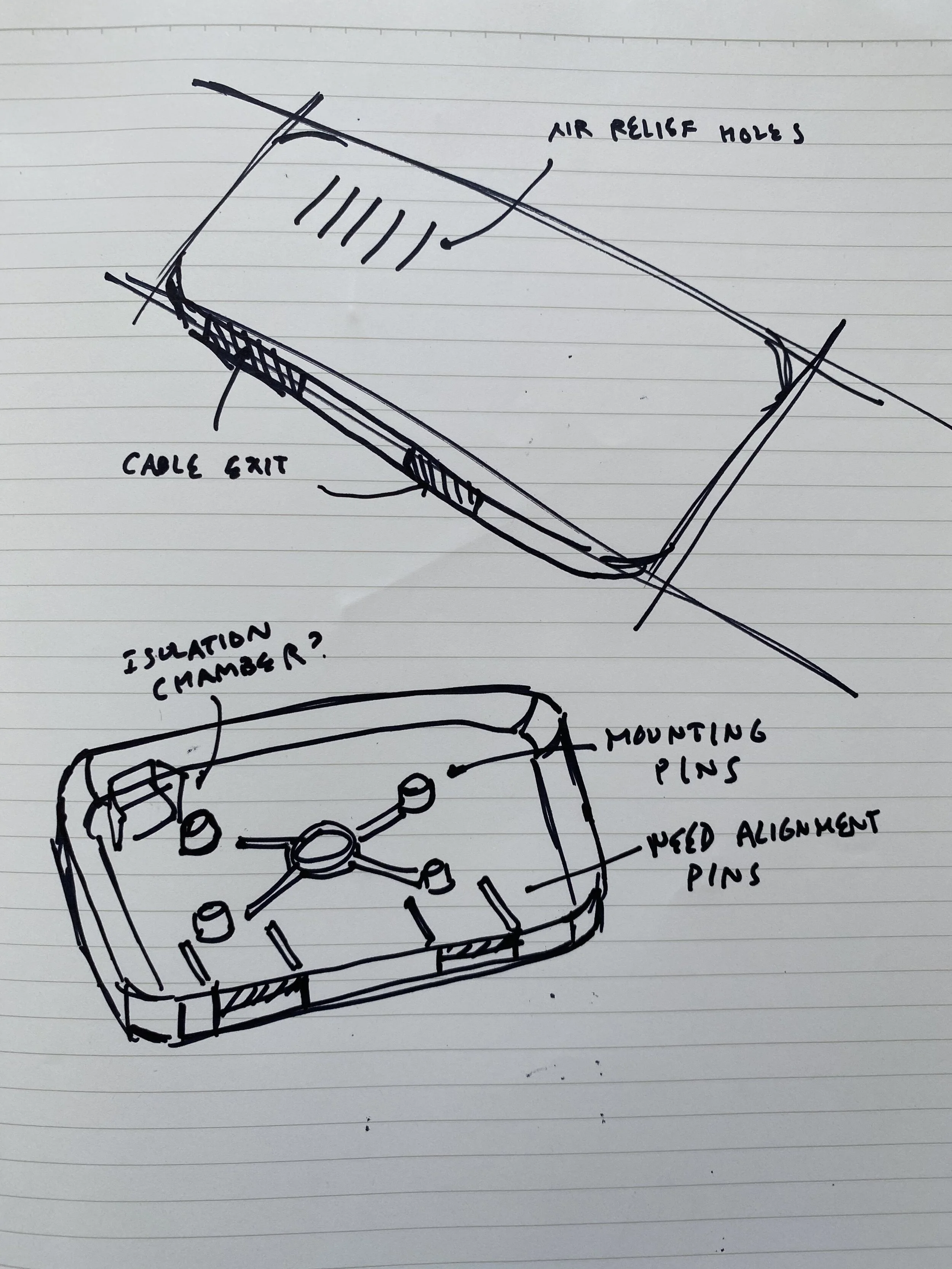
Several consumer containers, such as Clorox Wipes, were inspected for how they maintained an open and closed lid. Internal locking mechanisms were examined for a better understanding of a long term sealing solution.
Initial Design Sketch
INITIAL MANUFACTURING:
Using Form 3-D printers, several prototypes were made and fit tested with non populated boards with reference sizes and essential holes to ensure locking mechanisms worked. In addition, mock FPCB and cables were used to test for strain relief.
RE-DESIGN:
Although the housing fit the sensor board well, the PCB went through several design changes that shrank the over all dimensions and realigned the mounting features. Furthermore, the location of the key sensor that required isolation and ventilation also moved. As such, the PCB housing needed to be adjusted to match this new design.
MANUFACTURING:
Once all design changes were accepted, the newly designed components were 3-D printed and fit tested with the new mock boards. These boards held only the necessary mounting holes and alignment features.
CAD MODELS
Start to Finish: The CAD Process
Initial Top HOUSING design
Initial design was made to verify locking features and mounting hole locations, with the understanding that these may change. Furthermore, a keep out zone was built into the CAD in anticipation of isolating a sensor on the board.
iNITIAL BOTTOM HOUSING DESIGN
Initial design was made to verify cable and FPCB strain relief, with the understanding that these may change. Furthermore, a keep out zone was built into the CAD in anticipation of isolating a sensor on the board.
Final Bottom Housing Design
Final TOP HOUSING DESIGN
Final design of the PCB bottom housing to account for redesigned board layout. Keep out zone was changed into a circular module and cable stress relief features were added.
Final design of the PCB top housing to account for redesigned board layout. Keep out zone was changed into a circular module and cable stress relief features were added.
FUTURE
Design has been implemented and the manufacturing process has begun. This housing will be part of a new product launch.


